HORIBA 法國原廠於2021年6月24日舉辦的VIP網路會議討論了拉曼光譜儀在半導體尺寸測量領域中的重要性。
完整的webinar請在此連結觀看: https://www.horiba.com/en_en/products/scientific/recordedwebinars/raman-spectroscopy-for-dimensional-metrology-in-semiconductor-nano-electronics/
--------------------------------------------------------------------------------------
大綱:
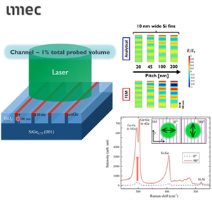
拉曼光譜是研究半導體基本特性的強大的工具,拉曼在合金的平均成份分析、機械應力變化、結晶品質及平均參雜級是特別的靈敏,對於建立微電子元件的特性上十分有效,拉曼光譜提供的資訊對於校準材料的生長過程以及監控他們的的電子與光學特性是必須的。
這場線上會議,由比利時的Thomas Nuytten介紹拉曼光譜在半導體尺寸測量領域中的重要性,他的研究顯示偏振拉曼可以觀察數十奈米線的結構,他舉例顯微拉曼的優點:速度、非破壞性量測、良好的空間解析度與深度量測能力,來說明拉曼從實驗室到晶圓廠的改變。
Raman spectroscopy is a powerful tool for investigating the basic properties of semiconductors. It is particularly efficient in establishing the characteristics of microelectronic devices as Raman is sensitive to the average composition of alloys, mechanical stress, crystalline quality, and average doping level. All the information provided by Raman spectroscopy is essential for the calibration of growth processes and the control of the electrical and optical behavior of these materials.