
突破極限:半導體與二維材料分析新視野
Pushing Boundaries in Semiconductor and 2D Materials Analysis
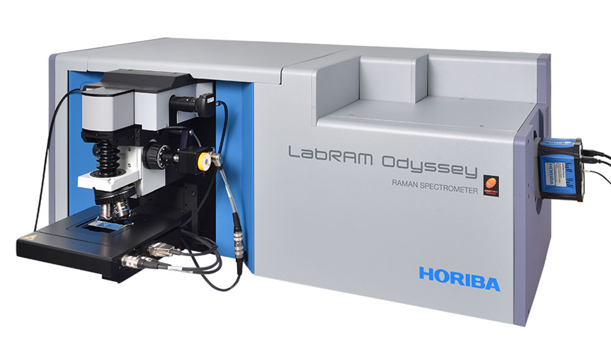
HORIBA LabRAM Odyssey 共軛焦拉曼暨高解析光譜儀,具備先進材料研究所需的極致精度,光譜解析度可達 0.1 cm⁻¹,並具備低於 5 cm⁻¹ 的超低頻(ULF)截止能力。如此高性能表現,對於觀測半導體與二維材料中細微的拉曼位移至關重要,能有效揭示應變、缺陷與層間動態等關鍵訊息。
The HORIBA LabRAM Odyssey Confocal Raman & High-Resolution Spectrometer delivers the precision needed for advanced materials research, with spectral resolution down to 0.1 cm⁻¹, and Ultra Low Frequency (ULF) cutoff less than 5 cm⁻¹. This level of performance is critical for detecting the subtle Raman shifts that reveal strain, defects, and interlayer dynamics in semiconductors and 2D materials.
高光譜解析度:解析矽(Si)、碳化矽(SiC)、鑽石與氮化鎵(GaN)等半導體材料的結構細節
|
•製程中產生的殘留應力 • 外延成長中的應變鬆弛現象 • 缺陷與聲子侷限效應 • Residual stress from processing |
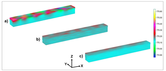
 Application Note: False color 3D view (below surface) of fitted E2 peak positions of the (a) as-cut SiC sample (b) diamond-lapped SiC sample and (c) CMP polished SiC sample. |
超低頻偵測能力:揭示石墨烯與TMDs層間相互作用
|
• Shear/layer-breathing mode analysis • Detection of near-Rayleigh lattice vibrations • Identification of heterostructure strain and stacking |

|


